
2017
8 JunUCSI’s engineering students visits MIMOS Semiconductor (M) Sdn Bhd

Kuala Lumpur: UCSI University's Electrical and Electronics Engineering department under the Faculty of Engineering, Technology and Built Environment recently organised an industrial visit trip to MIMOS Semiconductor (M) Sdn Bhd. The visit was organised by the Institute of Electrical and Electronics Engineers Eta Kappa Nu Mu Alpha chapter (IEEE – HKN) in collaboration with UCSI IET On Campus and IEEE Instrumentation and Measurement Malaysia Chapter.
The visit aims to provide students from the Electrical and Electronics Engineering programme, especially from the VLSI Design course, genuine hands-on industry exposure on semiconductor technology and IC design fabrication process at the MIMOS Wafer Fab. MIMOS Wafer Fab is MIMOS Berhad’s first research and development (R&D) facility commenced operation in 1997 and is currently dedicated to R&D in microelectronics systems (MEMS) and nanotechnology.
During the visit, students were exposed to a wide range of industrial testing equipment, wafer fabrication processes and testing techniques. The one-day training began with an introduction of semiconductor testing, test development and characterisation. This allowed the students to familiarise themselves with the semiconductor and testing modules throughout the course.
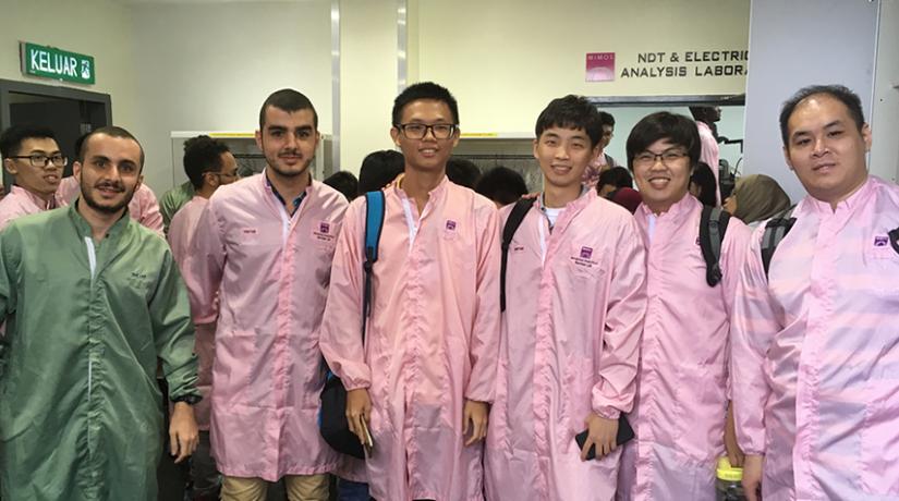
The students also visited the MIMOS Non-destructive testing (NDT) and Electrical Analysis Laboratory where they were given hands-on experience in different manufacturing and fabrication processes of semiconductor technology, wafer chip testing, IC design and reliability testing.
The visit is part of the University’s industry engagement activities and students can look forward to more opportunities to relate theory to industry application.

